
 Edito : "Nanoelectronic research: the next step"
 What Does the Future Hold for the Microelectronics Industry?
 REMINDER miniaturizes volatile memory
 Nanonet sensors for patients?
 Download newspaper
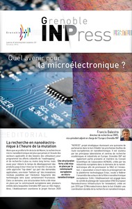
 Nanoelectronic research: the next step
 As we reach the end of Moore’s Law, research in micro and nanoelectronics is all the more focused on user needs and concrete applications. The industry is encouraging collaborative roadmapping that will enable both long term research and shorter development cycles to accelerate time to market for new products. In addition to a top-down approach that stems from concrete needs, there is also a bottom-up approach growing out of the many technological innovations that have opened the door to incredible advances. The industry has strong and organized backing from the European community, including several institutions tied to Grenoble INP. The school is coordinating the Horizon 2020 NEREID project, which is a strategic initiative to unite 15 partners and establish the future European roadmap for nanoelectronics research. The project is supported by the leading European laboratories and research centers. Grenoble INP is also a member of the AENEAS association’s Science Committee. The association was created by European nanoelectronics companies to promote R&D and innovation. It is an extension of the Eniac technology platform, which aims to unite all European nanoelectronics players. Finally, the school has join the European Nanoelectronics Infrastructure for Innovation, which was created STMicroelectronics in 2010 to encourage sustainable nanoelectronics research over the short and long term with all types of actors (academic research for the long term, research institutes for the middle term, and industrial players for the short term).
Francis Balestra
Director of Research at the CNRS
Grenoble INP Deputy Vice-President in charge of Europe

What Does the Future Hold for the Microelectronics Industry?
The micro and nanoelectronics industry is at a turning point in its history. To continue being competitive, it has to innovate at all levels. Grenoble INP is working hand in hand with the industry’s players to build a new future, in particular thanks to European projects.
Moore’s Law has guided the digital revolution for the past 40 years. For decades, the microelectronics industry focused on miniaturization and increasing speed. However, the time has come for the industry to reinvent its approach to electronics and find itself a new set of goals.
The limits of physics
It had to happen sooner or later. Miniaturization has hit concrete barriers in phsyics. As a result, innovation to increase the performance of integrated circuits must now come from new materials and architectures. Several paths are being explored by Grenoble INP laboratories, including new concepts for transistor and circuit architectures or logic elements.
Grenoble INP is also participating in several European projects to develop memory solutions. For example, the Spintec laboratory is collaborating on the European SPOT project and working to develop innovative spintronics-based memory.
Other laboratories are exploring alternatives to silicon, which has reached its limit. Many materials are being considered, but for the moment none have evolved past the phase of a lab prototype. Materials currently being explored include germanium, graphite, other 2D materials such as Transition Metal Dichalcogenide, SiC and carbon nanotubes.
While we wait for new innovations to emerge from laboratories, scientists are also working to improve the impact and sustainability of current technology. “For example, we’re working on finding alternatives for rare or toxic materials. We’re also looking to reduce energy consumption for components and circuits, which is a major factor for IoT applications.” explains Francis Balestra, coordinator of the European NEREID project.
Grenoble INP has a strong history with low-energy integrated circuits, which were first developed in one of its laboratories in the 80s. In combination with Fully Depleted Silicon on Insulator technology (FD-SOI) and Fully Inverted components, these technologies enable the production of low-consumption, high-performing circuits. In particular, they lower leakage rates which enables further integration. FD-SOI technology is also compatible with current design and production processes. As this technology has reached maturity, it continues to be deployed as part of European projects such as the ECSEL project, of which Grenoble INP is a partner.
Working towards micro-nanosystems
Current CMOS technology, which enables calculation and memory, is not sufficient to further microelectronics development. In response, the idea is to develop “More than Moore” by reversing the approach and starting from concrete needs in order to find solutions.
“The fields of energy, transportation, health, security, IoT, mobile applications and industrial production all have growing needs for nanoelectronics. General technology and designs can be used, but each industry has increasingly specific requirements for a wide array of applications.”
The idea is to add functions to a circuit using components such as sensors, switches, radio communications, power electronics, energy recuperation, imaging, lighting, etc. This enables the creation of micro-nanosystems capable of accomplishing complex tasks.
Chips can also be improved thanks to the use of 3D integration which superimposes several chips in order to create more powerful components with new functionalities all the while maintain an almost identical size. Other promising areas include the integration of heterogeneous chip functionalities using various technologies and materials.
By associating “more Moore” and “more than Moore”, CMOS technology has many opportunities to grow. However, at one point or another, the technology will still hit physical and economic barriers. As a result, the sector’s industrial and international scientific communities have been working to explore new options that go beyond CMOS technology and Moore’s Law. By introducing new concepts that do not rely on the traditional CMOS transistors and silicon-based microelectronics, it should be possible to develop less expensive options. Several possibilities includes spintronics, nanoelectromechanical structures, molecular electronics and quantum electronics.
Complementary laboratories
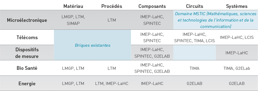
Grenoble’s laboratories include seven labs that are partnered with Grenoble INP. They all have a combination of experimental and theoretical skills that cover the entire field of research from materials to processes, components, circuits and systems. These skills enable them to contribute to numerous fields of activity in microelectronics such as logics, telecoms, physics measurements, biology, healthcare and energy.
REMINDER miniaturizes volatile memory
The goal of the European REMINDER project is to reduce the size of memory options without reducing their storage capacity. From a technical viewpoint, DRAM (or dynamic RAM) is made up of a transistor and a condensator in which information is stored as an electrical charge that has to be refreshed every couple of milliseconds.
Over the past ten years, the IMEP-LaHC has explored several revolutionary concepts to reduce the size of transistor/condensator combinations. “We focused on imagining memory concepts in which the capacity would simply be eliminated.” explains Maryline Bawedin, a professor at Grenoble INP-Phelma and a laboratory researcher.
These patented concepts were pre-selected for the European REMINDER project. The project unites several partners to find a revolutionary solution to overcome challenges in miniaturization. The idea is to increase the available space on circuits by having transistors stock and read information at the same time. “Thanks to SOI technology, which isolates each transistor, we can stock information in the form of an electrical charge without it leaking into the circuit.”
Finally, the concept that was selected for the project is an even more innovative idea that was developed and patented by Grenoble laboratories. This Z2-FET concept meets requirements in terms of low energy consumption for IoT objects. As part of the REMINDER project, researchers have to precisely define how they will stock and read information. They will then integrate the component within a complete demonstrator to test its operational capacities and see how it deals with technological constraints.
Nanonet sensors for patients?
The medical industry currently has needs for pre-diagnostic and monitoring sensors that can be used at a patient’s beside. One promising solution could be to use nanowires which are highly sensitive to anything that modifies their surface. However, integrating them in a CMOS system requires costly technology. This has slowed their development.
However, could provide a cheaper solution to integrate and use nanowire technology. In addition, Grenoble INP holds the patent for a sintering technique that helps ensure the nanonet’s cohesion, increases its conductivity and improves its adherence to the substrate.
To prove the validity of this idea, the Nanonets2sense project aims to produce two demonstrators that will detect two types of molecules: first, a molecule found in abundance in the breath of diabetic patients during hypoglycemic shock, and second, a DNA detection model to monitor signs of cancer development in the blood. Started in February 2016, the project has delivered its first results and will last for three years.
 Top (contents)
 Download the newspaper