A new state-of-the-art scientific instrument arrives in Grenoble

A latest-generation PFIB-SEM,* funded by Grenoble INP-UGA and the French Alternative Energies and Atomic Energy Commission (CEA), has been inaugurated in Grenoble.

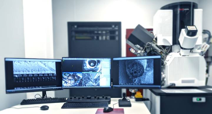
Traditionally used in the semiconductor industry, FIB-SEMs are seldom found in academic institutions and those based on plasma technology, as is the case with this new acquisition, are even rarer still. This instrument replaces the now obsolete device purchased in 2009 via the Nanosciences Foundation, and reinforces Grenoble INP-UGA's collaboration with the CEA on this technique.

At the end of 2022, a state-of-the-art PFIB-SEM was installed on the Nanocaracterisation Platform (PFNC) at the CEA centre in Grenoble. Half of its total cost of €1,032,000 was funded by the CEA and the remainder by Grenoble INP-UGA, with support from Labex CEMAM (Centre of Excellence for Multifunctional Architectured Materials).

Rarely encountered in academic environments, this scientific instrument combines a focused ion beam (FIB) with a scanning electron microscope (SEM) to enable the etching of matter at an accuracy exceeding 10 nm. In this case, a new xenon plasma technology replaces the formerly used gallium-ion-based system. "The new plasma technology increases ion abrasion speeds by up to a factor of 20 compared with a traditional gallium FIB, while limiting the phenomenon of ion implantation", explains Laurent Maniguet, Director of the CMTC** platform. “In practical terms, this means we can obtain cuts measuring several tens of microns across in a matter of minutes." The device can be used as a nanometric scalpel to incise matter, combined with an electron microscope to observe its properties.

PFIB-SEM 
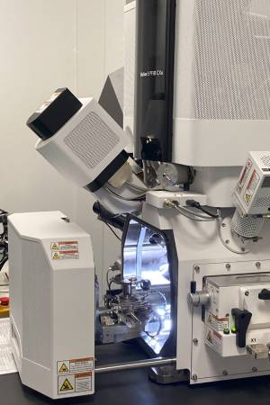
A wide range of applications
This tool is mainly used to manufacture thin slides (less than 100 nanometres thick) for transmission electron microscopy (TEM). This is particularly useful for the observation of architectured materials:  "observing the stacking of the different layers, measuring thicknesses and examining what is happening at the interfaces at a nanometric scale." At Grenoble INP-UGA, it will notably be used to prepare samples for crystallographic grain orientation mapping, using the ASTAR system developed by the SIMaP*** laboratory.
The second major application is 3D imaging. "PFIB technology enables us to cut successive slices less than 10 nm thick," explains Laurent Maniguet. An SEM image is acquired for each slice, and together these images can be used to reconstruct the volume in 3D with a high degree of precision." Finally, the PFIB microscope will be used to locally abrade material and enable its observation beneath the surface. This use, which is highly developed in the semiconductor industry, has been extended to materials and life sciences. Other applications include microfabrication and the nano-manipulation of objects.
The arrival of this instrument perfectly complements the range of 3D imaging instruments available on the Grenoble INP-UGA CMTC platform, in terms of the scales at which matter can be viewed. "PFIB-SEM is situated somewhere between X-ray tomography, which can be likened to a medical scanning device, and the atom probe, which has just arrived at SIMAP*** and enables the performance of 3D imaging at the atomic cluster scale." At Grenoble INP-UGA, this PFIB-SEM will be used by a number of Labex CEMAM partner laboratories such as SIMaP*** for developing additive manufacturing processes, LEPMI****, where it will contribute to the development of the batteries of the future, and LMGP***** for the design of nano-objects.

*Plasma Focused Ion Beam - Scanning Electron Microscope
**Consortium des Moyens Techniques Communs
***CNRS, UGA, Grenoble INP – UGA
****CNRS, UGA, Grenoble INP – UGA, USMB
****CNRS, Grenoble INP – UGA