Accueil - Home
One dimensional (1D) nanostructures such as nanotubes (NTs) or nanowires (NWs) have been attracting a large interest in the last decades. These 1D nanomaterials exhibit interesting electrical, optical, mechanical and chemical properties thanks to their high aspect ratio and large surface area. Because of their surface properties, NWs have been developed in many applications such as solar cells, biological and chemical sensors, catalysts or batteries. However, due to time consuming, complex and expensive technological techniques, the industrialization of devices based on a unique NWs is limited. Moreover, due to a large variability between NW properties, there is an obvious lack of reproducibility from one device to another. As a consequence, it is difficult to exploit unique properties of NWs into actual devices.
On the contrary, materials composed of randomly oriented NWs offer a good reproducibility and have been attracting recent interest in many applications. Also called “nanonets”, for NANOstructured NETworks as proposed by G. Grüner, such materials show several interesting properties arising either from the individual components, the NWs or NTs, or from the structural properties of the network itself. These properties include:
- High surface area/high porosity. Due to the component geometry, the surface area drastically increases, in comparison with thin films. As a consequence, addition of functional materials is favored due to the high porosity.
- Electrical conductance. The so-defined nanonets are above the percolation threshold and the larger the NW conductivity, the better the network conductance. Factors like NW-NW contacts are playing a major role and have to be studied and optimized.
- Optical transparency. A network of high aspect ratio nanostructures has high transparency approaching 100% when aspect ratio tends to infinity. However, when dealing with absorbing materials, the transparency decreases when aspect ratio decreases.
- Mechanical robustness and flexibility. A random network of interwoven NWs has significantly higher flexibility than that of a thin film.
- Reproducibility and fault tolerance. At the macroscopic scale, the nanonet involves several millions of NWs so that the observed properties result from a large scale statistical averaging on individual NW properties. Moreover, breaking a conducting path in the network leaves many others still present and the overall properties of the nanonet are stable. As a consequence, in contrast to individual components, nanonets offer high reproducibility of the physical properties coupled with easy preparation.
- High quality components. It is easy to grow defect free NWs over large area so that the electrical and optical properties are improved
- Functionalization ability. By attaching chemical species or nanoscale materials such as nanoparticles (NPs) with well-defined functionality, it is possible to add properties induced by the synergy between NWs and NPs.
When the nanonet thickness is significantly thinner than the length scale of its individual components, the nanonet is considered as two-dimensional (2D) because the percolation properties of such network show typical 2D characteristics. Carbon nanonets (composed of carbon NTs, functionalized or not) and metallic nanonets (composed of silver or copper NWs) have been studied for a decade and are widely described in the literature particularly for the fabrication of transparent and conductive thin films for photovoltaic applications. In contrast, there are currently very few studies on 2D nanonets based on nanomaterials other than carbon or silver, such as, for example, Si, ZnO, and other semiconducting NWs, despite the high potential of such materials.
From Serre et al, Nanotechnology 26 (2015) 015201
Carbon nanonet combined electrical conductance and optical transparency (from C. Aguire PhD Thesis)
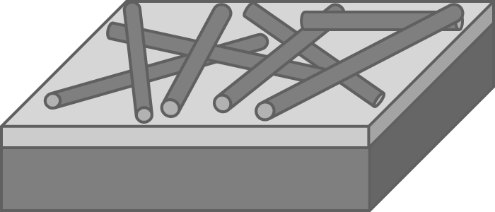
2D nanonets
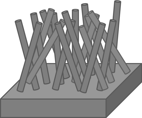
3D nanonet
Related Website
Si Nanonets
Composed of Si nanowires (NWs), Si nanonets are, so far, considered by the scientific community as non-interesting material for electrical applications. For example, Hong wrote in one of his highly cited paper: “One of the major problems in using Si-NWs for large area device applications is that it is very difficult to build long-channel devices based on Si-NW networks because individual Si-NWs do not make a good electrical contact with each other due to the native oxide layer. A possible solution is putting intermediate contact pad structures on long Si-NW network channels.” [Nano Letters 8 4523–7 (2008)].
We demonstrate that using adequate processing, it is possible to build percolating networks that show high and long-term performances.
ZnO Nanonets
Composed of ZnO nanowires (NWs), ZnO nanonets are the last came for us. They are very promising materials in numerous fields as ZnO is a wide band gap semiconducting material, with interesting wettability and photocatalysis properties. It is piezoelectric, is biocompatible, non-toxic and largely available on the earth. ZnO nanonets are highly promising in the field of detection, of both bio-chemical species and light. Presently, we are working on aspect ratio (length over diameter) otpimization of ZnO NWs grown by wet chemistry. Indeed, high aspect ratios (>50) are mandatory to increase nanonet homogeneity and small diameters (<50nm) are required to enhance detection ability.
Si Nanonets
What has been achieved:
- precise monitoring of the Si nanonet morphology
- easy functionalization for DNA grafting
- enhanced hybridization detection by fluorescence
- develop integration scheme
- understanding the mechanisms involved in the nanonet conduction for n-degenerated Si nanowires
- study the percolation behavior of the degenerated Si nanonets
- stabilize the electrical properties over months, even in oxidizing atmosphere
What is under study:
- electrical behavior of low-doped Si nanonets
- electrical detection of DNA hybridization
- above IC integration scheme
Bibliography:
- "First evidence of superiority of Si nanonet field effect transistors over multi-parallel Si nanowire ones in view of electrical DNA hybridization detection." Nguyen, T.T.T., Legallais, M., Morisot, F., Cazimajou, T., Stambouli-Sene, V., Mouis, M., SALEM, B., & Ternon, C. Materials Research Express 6 016301 (2019)
- "Electrical characteristics of silicon percolating nanonet-based field effect transistors in the presence of dispersion" T Cazimajou, M Legallais, M Mouis, C Ternon, B Salem, G Ghibaudo, Solid-State Electronic 143, 83-89 (2018)
- "An innovative large scale integration of silicon nanowire-based field effect transistors", M Legallais, TTT Nguyen, M Mouis, B Salem, E Robin, P Chenevier, C. Ternon, Solid-State Electronics 143, 97-102 (2018)
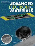
- “Silicon Nanowires: Low Temperature Processing to Form Oxidation Insensitive Electrical Contact at Silicon Nanowire/Nanowire Junctions “, Céline Ternon, Pauline Serre, Jean-Marie Lebrun, Virginie Brouzet, Maxime Legallais, Sylvain David, Thierry Luciani, Céline Pascal, Thierry Baron andJean-Michel Missiaen, Adv. Electron. Mater. 10 (2015)
- “Percolating silicon nanowire networks with highly reproducible electrical properties “, P. Serre, M. Mongillo, P. Periwal, T. Baron, and C. Ternon, Nanotechnology 26, 015201 (2015)
- “High aspect ratio semiconducting nanostructure random networks: highly versatile materials for multiple applications”, Céline Ternon, Pauline Serre, Germain Rey, Claire Holtzinger, Priyanka Periwal, Mickaël Martin, Thierry Baron, Valérie Stambouli, and Michel Langlet, Phys. Status Solidi RRL 7, 919–923 (2013)
- “Fabrication of silicon nanowire networks for biological sensing”, P. Serre, C. Ternon, V. Stambouli, P. Periwal and T. Baron, Sensors and Actuators B 182, 390-395 (2013)
Talking about us:
- Eclairages (2016)
- Advances in Engineering (2015)
- Minanews (2015)
- Nanotechweb (2014)
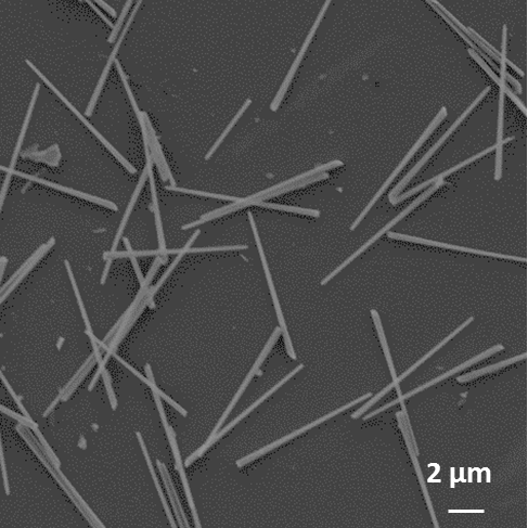
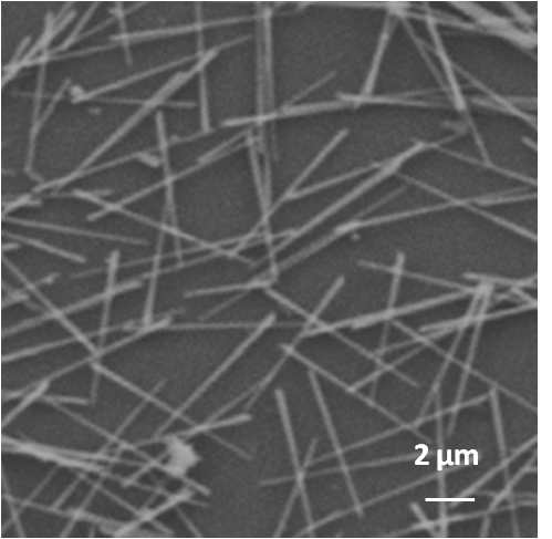
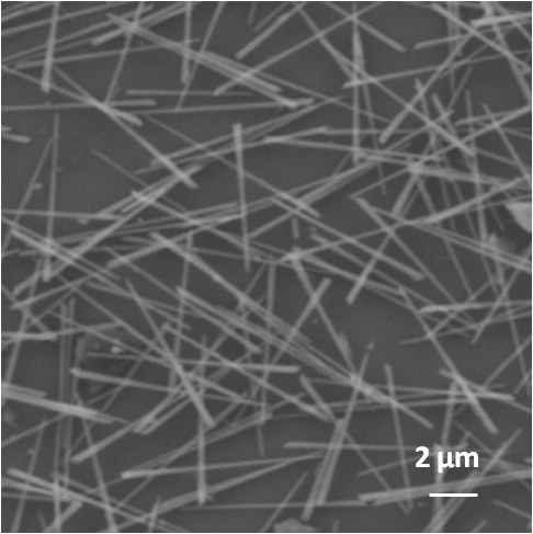
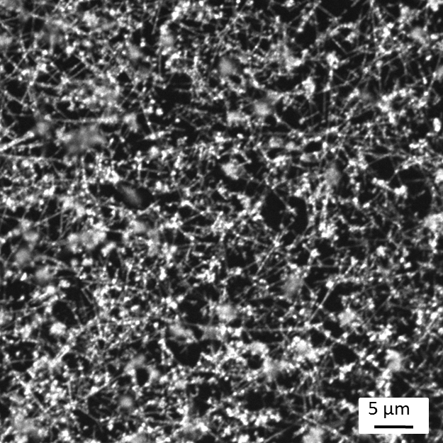
Si nanonets with increasing NW density
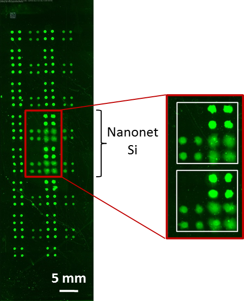
DNA biochip based on Si nanonet - Fluorescence localized on Si NWs
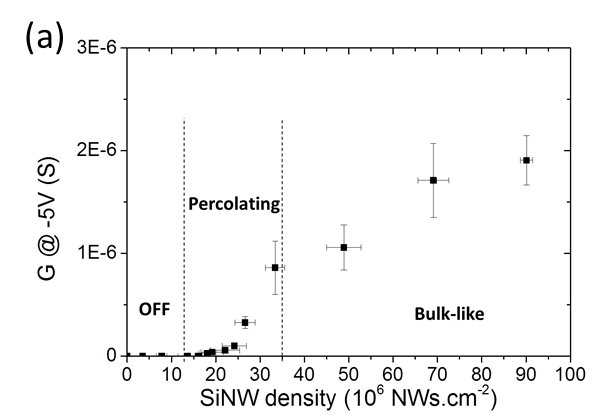
Various electrical regime depending on SiNW density
DNA biochip based on Si nanonet - Fluorescence localized on Si NWs
Various electrical regime depending on SiNW density
ZnO Nanonets
What has been achieved:
- monitoring the ZnO nanowire diameter by wet chemistry growth
- monitoring the ZnO nanonet morphology
- stabilizing ZnO nanonets morphology and properties in air
- easy functionalization for DNA grafting
- acetone detection
What is under study:
- surface properties of ZnO nanonets
- monitoring the amount of DNA grafted on nanonet surface
- developing the integration scheme
- electrical properties
Bibliography:
- "Mechanisms involved in the hydrothermal growth of ultra-thin and high aspect ratio ZnO nanowires", C. Ternon, T. Demes, F. Morisot, D. Riassetto, M. Legallais, H. Roussel, M. Langlet, two first authors equally credited, Applied Surface Science 410, 423-431 (2017)
- "Comprehensive study of hydrothermally grown ZnO nanowires", T. Demes, C. Ternon, D. Riassetto, V. Stambouli, M. Langlet, J. Mater. Sci. 51, 10652 (2016) (pdf)
- "New insights in the structural and morphological properties of sol-gel deposited ZnO multilayer films", T. Demes, C. Ternon, D. Riassetto, H. Roussel, L. Rapenne, I. Gélard, C. Jimenez, V. Stambouli, M. Langlet, J. Phys. Chem. Sol. 95, 43-55 (2016)
- “High aspect ratio semiconducting nanostructure random networks: highly versatile materials for multiple applications”, Céline Ternon, Pauline Serre, Germain Rey, Claire Holtzinger, Priyanka Periwal, Mickaël Martin, Thierry Baron, Valérie Stambouli, and Michel Langlet, Phys. Status Solidi RRL 7, 919–923 (2013)
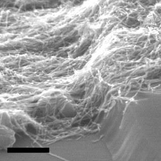
Highly flexible ZnO nanonets
(scale bar 500nm)
The nanonet composed of small diameter NW (~20nm)
is deposited over a step
Carbon Nanonets
This part of the work has been done in collaboration with R. Martel group initiated by a visiting period at Ecole Polytechnique de Montréal (2007). Coworkers were Carla Aguirre, Patrick Desjardins and Richard Martel.
What has been achieved:
- improving the conductivity by doping
- develop an original way of integration as top contact electrode for nanowire vertical assembly
- develop new design for electron injection in organic material
Bibliography:
- “Carbon nanotube sheet as top contact electrode for nanowires: highly versatile and simple process.” C. Ternon, F. Dupas, S. Stein, C. Aguirre, F. Dhalluin and T. Baron, J. Nanosc. Nanotech. 15, 1669-1673 (2015)
- “Carbon nanotubes as injection electrodes for organic thin film transistor devices”, C. M. Aguirre, C. Ternon, M. Paillet, P. Desjardins and R. Martel, Nanoletters, 9 (4) 1457-61 (2009).
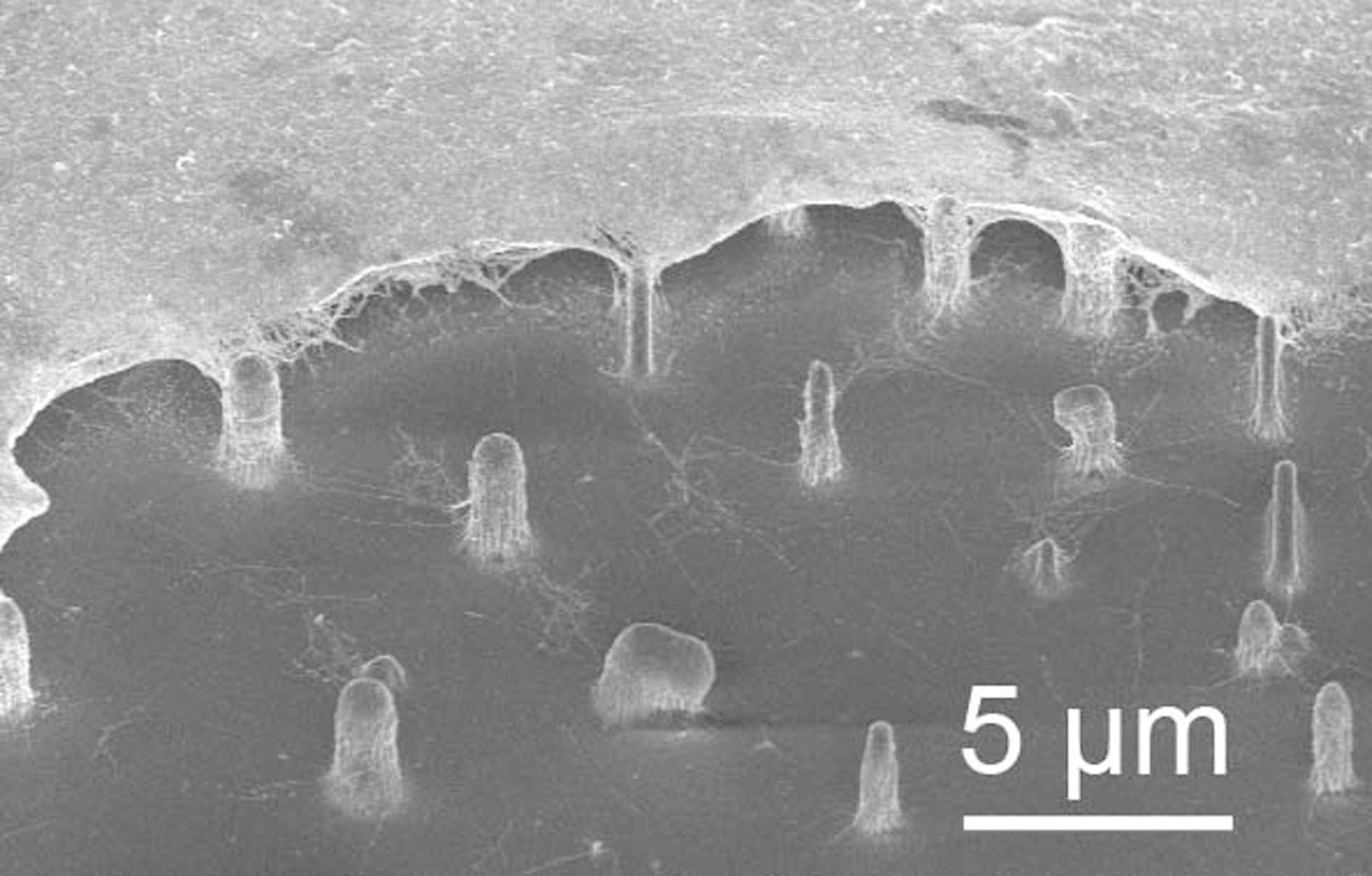
Carbon nanonet suspended on top of SiNW
Permanent Staff involved
David Riassetto, LMGP
Michel Langlet, LMGP
Bassem Salem, LTM
Valérie Stambouli, LMGP
Mireille Mouis, IMEP-LaHC
Michel Langlet, LMGP
Bassem Salem, LTM
Valérie Stambouli, LMGP
Mireille Mouis, IMEP-LaHC
Students
Tabassom Arjmand, PhD 2018-today
Monica Vallejo Perez, PhD 2017-today
Fanny Morisot, PhD 2016-today
Mariem Bourourou, Post-Doc 2019-today
Monica Vallejo Perez, PhD 2017-today
Fanny Morisot, PhD 2016-today
Mariem Bourourou, Post-Doc 2019-today
Alumni
Thuy Nguyen, Post-Doc 2017-2018
Maxime Legallais, PhD 2014-2017 and Post-Doc 2018
Thomas Demes, PhD 2013-2017
Pauline Serre, PhD 2011-2014
Trung Nguyen, Master thesis 2018
Hervé Palis, Master thesis 2013
Loic Gros, Master thesis 2012
Sergio Silveira-Stein, Master thesis 2010-2011
Florence Dupas, Master thesis 2009
Maxime Legallais, PhD 2014-2017 and Post-Doc 2018
Thomas Demes, PhD 2013-2017
Pauline Serre, PhD 2011-2014
Trung Nguyen, Master thesis 2018
Hervé Palis, Master thesis 2013
Loic Gros, Master thesis 2012
Sergio Silveira-Stein, Master thesis 2010-2011
Florence Dupas, Master thesis 2009